
Introduction to PIC
Introduction
Welcome to the start of the PIC Tutorial. These pages will take you form the basic structure of the device, right through to programming methods and techniques. Also, there will be suggestions on how to modify the code so that you can adapt the PIC to suit your applications within Cybot. We will not be including any internal architecture diagrams, as this may only lead to confusion. If you want to look at the datasheet, then this can be downloaded from Microchips' web site.
To start, let us take a look at the PIC.
Microchip PIC 16F84 Microcontroller
Microchip manufacture a series of microcontrollers called PIC. You can see the range of their microcontrollers here. There are many different flavours available, some basic low memory types, going right up through to ones that have Analogue - To- Digital converters and even PWM built in. We are going to concentrate on the 16F84 PIC. Once you have learnt how to program one type of PIC, learning the rest is easy.
There are several ways of programming the PIC - using BASIC, C, or Assembly Language. We are going to show you the Assembly Language. Don't be put off by this. There are only 35 instructions to learn, and it is the cheapest way to program the PICs, as you do not need any extra software other than the freebies.
The 16F84 Pins
Below is a diagram showing the pin-outs of the PIC 16F84. We will go through each pin, explaining what each is used for.
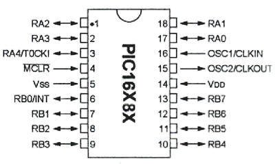
RA0 To RA4
RA is a bidirectional port. That is, it can be configured as an input or an output. The number following RA is the bit number (0 to 4). So, we have one 5-bit directional port where each bit can be configured as Input or Output.
RB0 To RB7
RB is a second bidirectional port. It behaves in exactly the same way as RA, except there are 8 - bits involved.
VSS And VDD
These are the power supply pins. VDD is the positive supply, and VSS is the negative supply, or 0V. The maximum supply voltage that you can use is 6V, and the minimum is 2V
OSC1/CLK IN And OSC2/CLKOUT
These pins is where we connect an external clock, so that the microcontroller has some kind of timing.
MCLR
This pin is used to erase the memory locations inside the PIC (i.e. when we want to re-program it). In normal use it is connected to the positive supply rail.
INT
This is an input pin which can be monitored. If the pin goes high, we can cause the program to restart, stop or any other single function we desire. We won't be using this one much.
T0CK1
This is another clock input, which operates an internal timer. It operates in isolation to the main clock. Again, we won't be using this one much either.
A Simple Development Board
Ok, so you have now got your programmer, and you have a PIC or two. It is all very well knowing how to program the PIC in theory, but the real learning comes when you try your code on a PIC and see the results yourself in a circuit.
You could build a circuit each time and program the PIC to see if the program works, or you can make yourself a development board. A development board allows you to simulate the environment around the PIC. We have included a circuit diagram to show a very basic and cheap development board. You can, of course add LEDs and switches to this, but We have included the bare bones. You can monitor the Input/Output pins by connecting LEDs directly to the pins, and they will light up when the pins go high. Also, you can add switches to the pins, so that you can select which inputs are high, and which are low. Basically, what We are saying is if you start with this circuit, you can add whatever you feel necessary.

We will run through the circuit diagram, which We admit isn't much, but it will give you a feel of things to come.
The supply rail is set to +6V, which is the maximum voltage of the PIC. You can use any voltage below this right down to +2V. C3 is known as a 'Bypass' Capacitor. All C3 does is reduce any noise on the supply rail. X1 is a 4MHz crystal. You could use a parallel resistor and capacitor circuit, but the cost of the crystal is negligible, and it is more stable. C1 and C2 help reduce any stray oscillations across the crystal, and get rid of any unwanted noise etc before the signal goes into the PIC
Before we get to the nitty gritty of programming the PIC, I think now is a good time to explain some good programming techniques.
If you type a ; (semicolon) anywhere in your program, the compiler will ignore anything after it until the carriage return. This means we can add comments in our program to remind us of what on earth we were doing in the first place. This is good practice, even for the simplest programs. You may well fully understand how your program works now, but in a few months time, you may be scratching your head. So, use comments wherever you can – there is no limit.
Secondly, you can assign names to constants via registers (more about these later). It makes it far easier to read in English what you are writing to, or what the value is, rather than trying to think of what all these numbers mean. So, use real names, such as COUNT. Notice that we have put the name in capitals. This makes it stand out, and also means that (by convention) it is a constant value.
Thirdly, put some kind of header on your programs by using the semi-colons. An example is below:
;;;;;;;;;;;;;;;;;;;;;;;;;;;;;;;;;;;;;;;;;;;;;;;;;;;;;;;;;;;;;;;;;;;;;;;;;;;;;;;;;;;;;
; Author : ;
; Date : ;
; Version: ;
; Title: ;
; ;
; Description: ;
; ;
; ;
; ;
; ;
; ;
; ;
; ;
; ;
; ;
;;;;;;;;;;;;;;;;;;;;;;;;;;;;;;;;;;;;;;;;;;;;;;;;;;;;;;;;;;;;;;;;;;;;;;;;;;;;;;;;;;;;;
; Author : ;
; Date : ;
; Version: ;
; Title: ;
; ;
; Description: ;
; ;
; ;
; ;
; ;
; ;
; ;
; ;
; ;
; ;
;;;;;;;;;;;;;;;;;;;;;;;;;;;;;;;;;;;;;;;;;;;;;;;;;;;;;;;;;;;;;;;;;;;;;;;;;;;;;;;;;;;;;
Notice that We have made a kind of box by using the semi-colons. This just makes it look neat.
Finally, try and document the program on paper as well. You can either use flow charts or algorithms or anything else you want. This will help you in writing your program, step by step.
Right, that’s the lecture over with, lets move on to the real stuff
The Registers
A register is a place inside the PIC that can be written to, read from or both. Think of a register as a piece of paper where you can look at and write information on.
The figure below shows the register file map inside the PIC16F84. Don’t worry if you haven’t come across anything like this before, it is only to show where the different bits and pieces are inside the PIC, and will help explain a few of the commands.
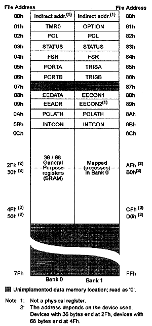
First thing you will notice is that it is split into two - Bank 0 and Bank 1. Bank 1 is used to control the actual operation of the PIC, for example to tell the PIC which bits of Port A are input and which are output. Bank 0 is used to manipulate the data. An example is as follows: Let us say we want to make one bit on Port A high. First we need to go to Bank 1 to set the particular bit, or pin, on Port A as an output. We then come back to Bank 0 and send a logic 1 (bit 1) to that pin.
The most common registers in Bank 1 we are going to use are STATUS, TRISA and TRISB. The first allows us to come back to Bank 0, TRISA allows us to select which pins on Port A are output and which are input, TRISB allows us to select which pins on Port B are output and which are input. The SELECT register in Bank 0 allows us to switch to Bank 1.
Let us take a closer look at these three registers.
STATUS
To change from Bank 0 to Bank 1 we tell the STATUS register. We do this by setting bit 5 of the STATUS register to 1. To switch back to Bank 0, we set bit 5 of the STATUS register to 0. The STATUS register is located at address 03h (the ‘h’ means the number is in Hexadecimal).
TRISA and TRISB.
These are located at addresses 85h and 86h respectively. To program a pin to be an output or an input, we simply send a 0 or a 1 to the relevant bit in the register. Now, this can either be done in binary, or hex. We personally use both, as the binary does help visualize the port. If you are not conversant with converting from binary to hex and vice versa, then use a scientific calculator.
So, on Port A we have 5 pins, and hence 5 bits. If We wanted to set one of the pins to input, We send a ‘1’ to the relevant bit. If We wanted to set one of the pins to an output, We set the relevant bit to ‘0’. The bits are arranges in exactly the same way as the pins, in other words bit 0 is RA0, bit 1 is RA1, bit 2 is RA2 and so on. Let’s take an example. If We wanted to set RA0, RA3 and RA4 as outputs, and RA1 and RA2 as inputs, We send this: 00110 (06h). Note that bit zero is on the right, as shown:
Port A Pin RA4 RA3 RA2 RA1 RA0
Bit Number 4 3 2 1 0
Binary 0 0 1 1 0
The same goes for TRISB.
PORTA and PORTB
To send one of our output pins high, we simply send a ‘1’ to the corresponding bit in our PORTA or PORTB register. The same format follows as for the TRISA and TRISB registers. To read if a pin is high or low on our port pins, we can perform a check to see if the particular corresponding bit is set to high (1) or set to low (0)
Before We give an example code, We need to explain just two more register – w and f.
W
The W register is a general register in which you can put any value that you wish. Once you have assigned a value to W, you can add it to another value, or move it. If you assign another value to W, its contents are overwritten.
An Example Code.
We are going to give you some example code on what we have just learnt. Don’t try and compile this yet, we will do that when we come to our first program. We are just trying to show how the above is actually programmed and introduce a couple of instructions along the way. We are going to set up Port A as per the example above.
First, we need to switch from Bank 0 to Bank 1. We do this by setting the STATUS register, which is at address 03h, bit 5 to 1.
BSF 03h,5
The BSF Means Bit Set F. The letter F means that we are going to use a memory location, or register. We are using two numbers after this instruction – 03h, which is the STATUS register address, and the number 5 which corresponds to the bit number. So, what we are saying is “Set bit 5 in address 03h to 1”.
We are now in Bank 1.
MOVLW b'00110'
We are putting the binary value 00110 (the letter b means the number is in binary) into our general purpose register W. We could of course have done this in hex, in which case our instruction would be:
MOVLW 06h
Either works. The MOVLW means ‘Move Literal Value Into W’, which in English means put the value that follows directly into the W register.
Now we need to put this value onto our TRISA register to set up the port:
MOVWF 85h
This instruction means “Move The Contents Of W Into The Register Address That Follows”, in this case the address points to TRISA.
Our TRISA register now has the value 00110, or shown graphically:
Port A Pin RA4 RA3 RA2 RA1 RA0
Binary 0 0 1 1 0
Input/Output O O I I O
Now we have set up our Port A pins, we need to come back to Bank 0 to manipulate any data.
BCF 03h,5
This instruction does the opposite of BSF. It means “Bit Clear F”. The two numbers that follow are the address of the register, in this case the STATUS register, and the bit number, in this case bit 5. So what we have done now is set bit 5 on our STATUS register to 0
We are now back in Bank 0.
Here is the code in a single block:
BSF 03h,5 ;Go to Bank 1
MOVLW 06h ;Put 00110 into W
MOVWF 85h ;Move 00110 onto TRISA
BCF 03h,5 ;Come back to Bank 0
Read this through a couple of times, until it is you can follow it. So far we have looked at 4 instructions. Only 31 to go!


